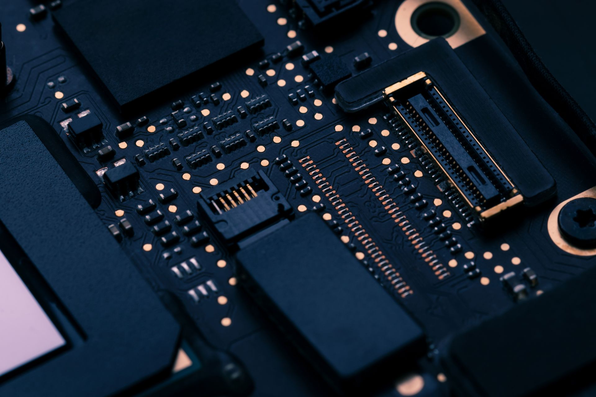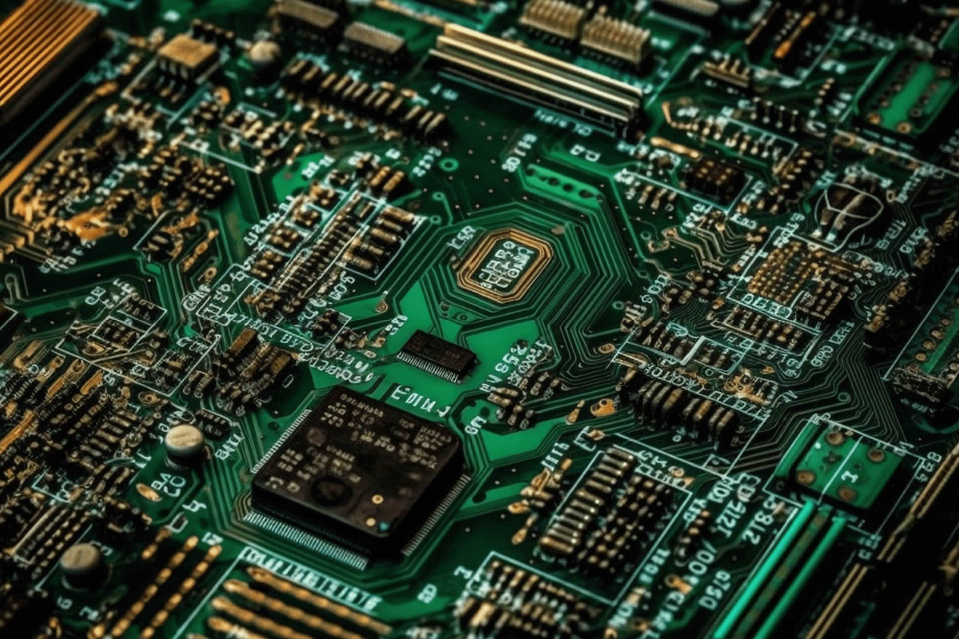
The process and steps involved in PCB (Printed Circuit Board) manufacturing typically include:
Circuit Design: Create circuit diagrams and layout designs using circuit design software (such as Altium Designer, Eagle, etc.) to determine the connections, component placements, and routing of the PCB.
Prototype Production: Produce a prototype PCB based on the design files. This can be achieved through two methods:
a. Software-generated Production: Export the design files into Gerber file format and send them to a PCB manufacturer who uses automated equipment to produce the PCB.
b. Handcrafted Production: Transfer the circuit diagrams and layout designs onto a copper-clad substrate using specialized PCB design software or transfer techniques like toner transfer.
PCB Material Preparation: Select suitable PCB materials (such as fiberglass-reinforced epoxy, FR-4), and cut them to the required dimensions.
Cleaning and Pre-treatment: Clean the PCB materials to remove any dirt, grease, and surface oxidation. Next, perform pre-treatment such as surface roughening, removal of protective films, etc., to facilitate better adhesion of coatings and printing processes.
Photolithography: Apply a photosensitive resist (photoresist) onto the PCB and transfer the resist onto the areas that require copper plating through exposure and development steps. The unprotected areas will be etched away.
Etching: Immerse the PCB in an etchant solution to remove the unprotected copper, creating the circuit traces and pathways.
Metalization Treatment: Protect the circuit traces by depositing a layer of metal (such as tin plating) onto the PCB's surface, providing a solderable surface.
Resist Removal: Remove the photoresist using chemical solvents or mechanical methods, exposing the solder pads where electronic components will be connected.
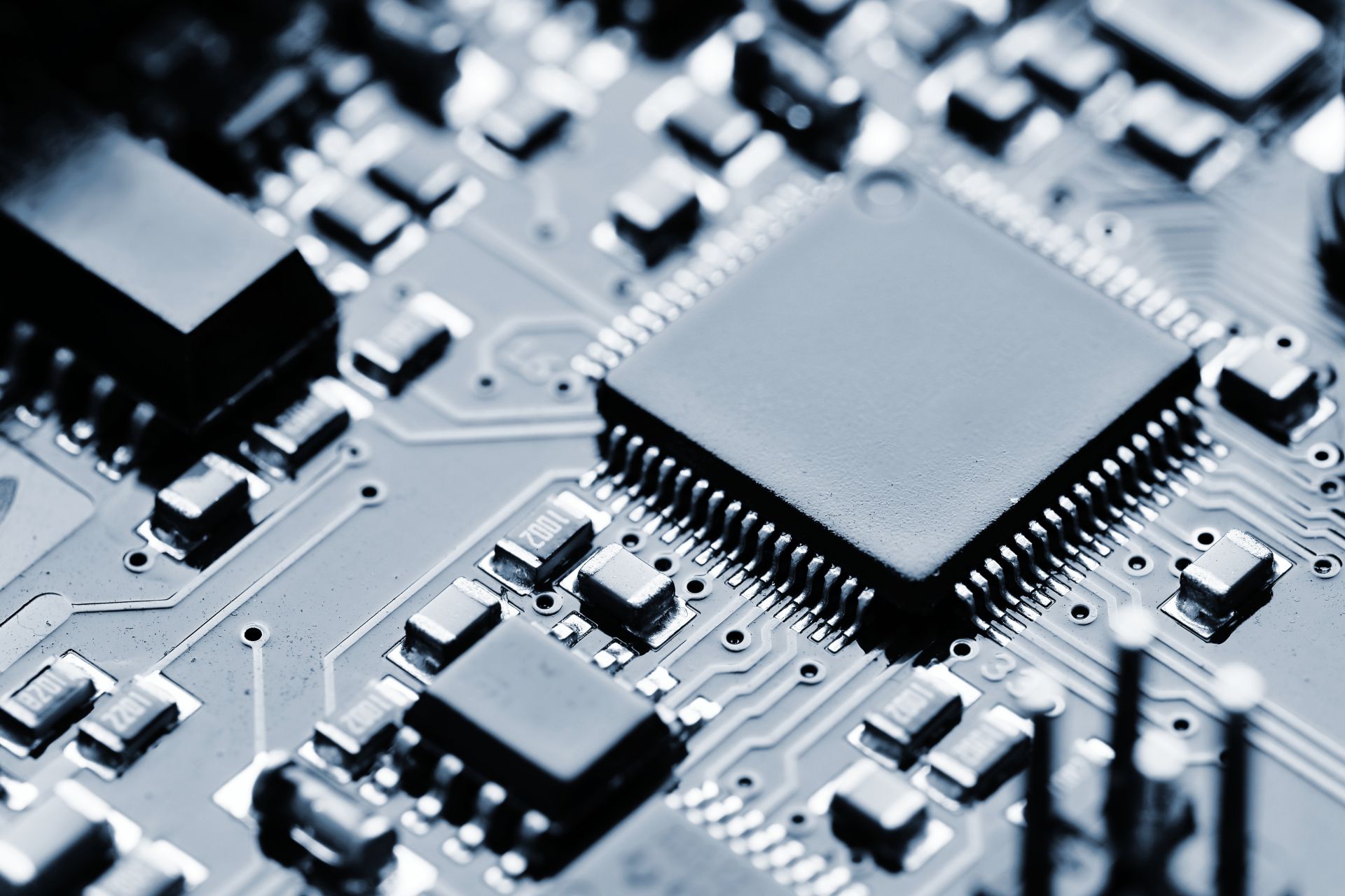
Component Assembly: Mount electronic components (such as resistors, capacitors, integrated circuits, etc.) onto the solder pads and connect them to the PCB using soldering techniques (manual soldering or surface mount technology).
Soldering: Join the components to the PCB by heating solder material (such as solder paste or solder wire), forming strong connections.
Cleaning and Coating: Clean the PCB to remove solder residues and contaminants. Optionally, apply a protective coating (such as conformal coating) to safeguard the PCB against environmental factors and enhance its reliability.
Testing and Inspection: Perform various tests, including electrical testing, in-circuit testing (ICT), functional testing, and visual inspection, to ensure the functionality, quality, and reliability of the assembled PCB.
Packaging and Finalization: Package the PCB, including adding necessary markings, labels, and documentation. The PCB is then ready for integration into the final electronic product.
It's important to note that the specific manufacturing processes and steps may vary depending on the complexity of the PCB, manufacturing capabilities, and quality requirements.