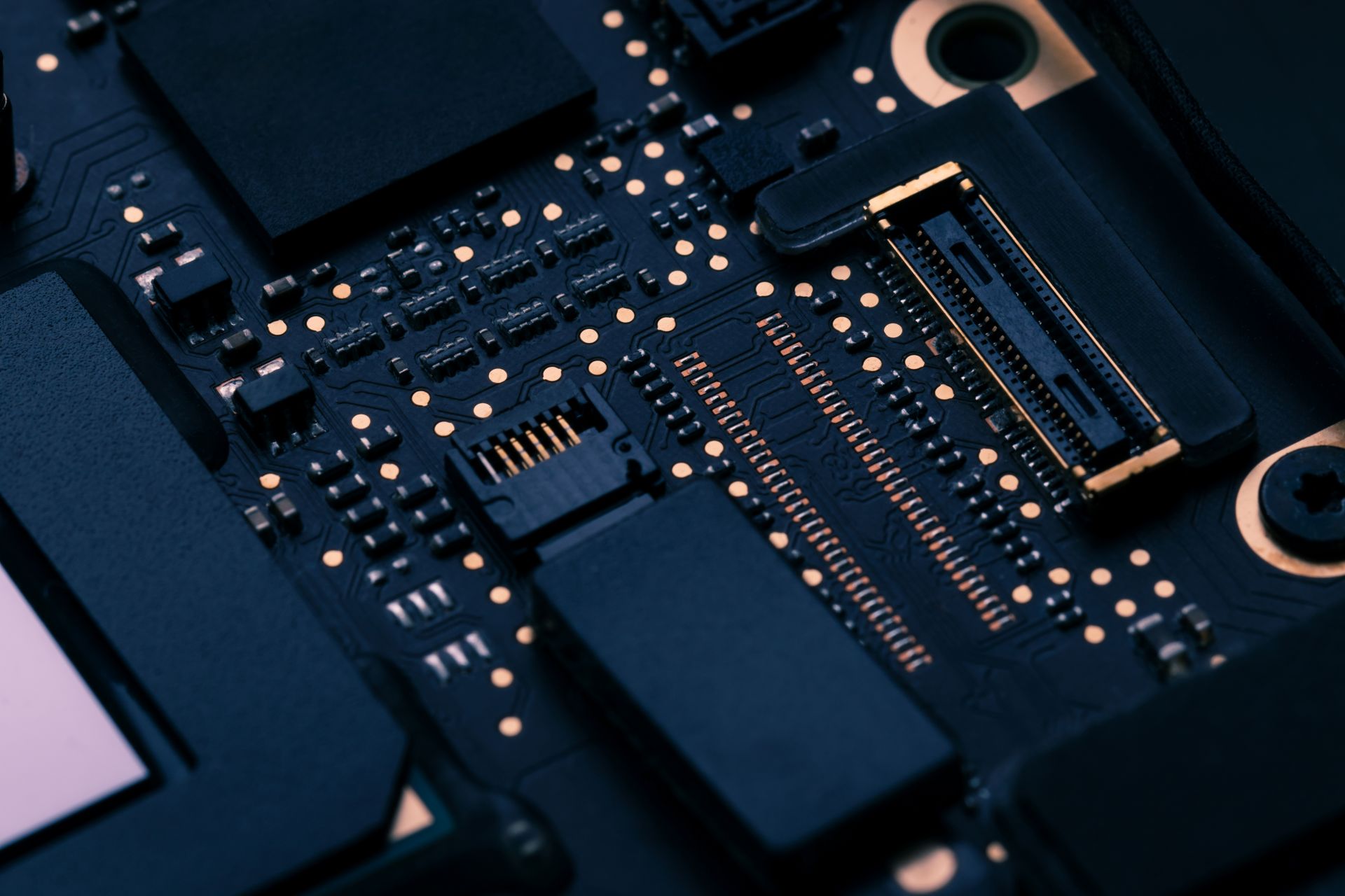
The advantages of HDI (High-Density Interconnect) PCB are as follows:
High-density routing: HDI PCB utilizes fine trace widths, spacing, and via structures to achieve higher circuit density. This makes HDI PCB particularly suitable for small electronic devices and high-performance electronic products as it allows for more functionality and complex circuit designs in limited space.
Size and weight reduction: Due to its higher circuit density, HDI PCB enables the reduction of board size and weight. This is crucial for compact design and lightweight devices such as mobile phones, laptops, tablets, etc.
Improved signal transmission performance: HDI PCB employs fine trace widths and spacing, which reduces signal propagation delay and loss. Additionally, by utilizing shorter circuit paths and minimizing electromagnetic interference, HDI PCB enhances signal integrity and noise immunity, thereby improving overall signal transmission performance.
Support for high-frequency applications: HDI PCB design effectively reduces signal crosstalk and electromagnetic leakage, providing better high-frequency performance. This makes HDI PCB highly suitable for high-speed communication, RF, and microwave applications, such as communication devices, wireless networks, radar systems, etc.
Enhanced reliability: HDI PCB design and manufacturing processes incorporate advanced techniques and materials such as blind vias, controlled impedance, multiple layer stack-ups, high-precision trace fabrication, etc. These features improve the reliability of the circuit board, reducing issues caused by thermal expansion, mechanical stress, and vibration.
Simplified assembly processes: The high-density routing and compact design of HDI PCB simplify the assembly process. By reducing distances between components and layer counts, HDI PCB improves assembly efficiency and lowers manufacturing costs.
In summary, the advantages of HDI PCB lie in its ability to provide higher circuit density, small size and lightweight form factor, excellent signal transmission performance, support for high-frequency applications, higher reliability, and simplified assembly processes. These factors make HDI PCB an ideal choice for many advanced electronic products.