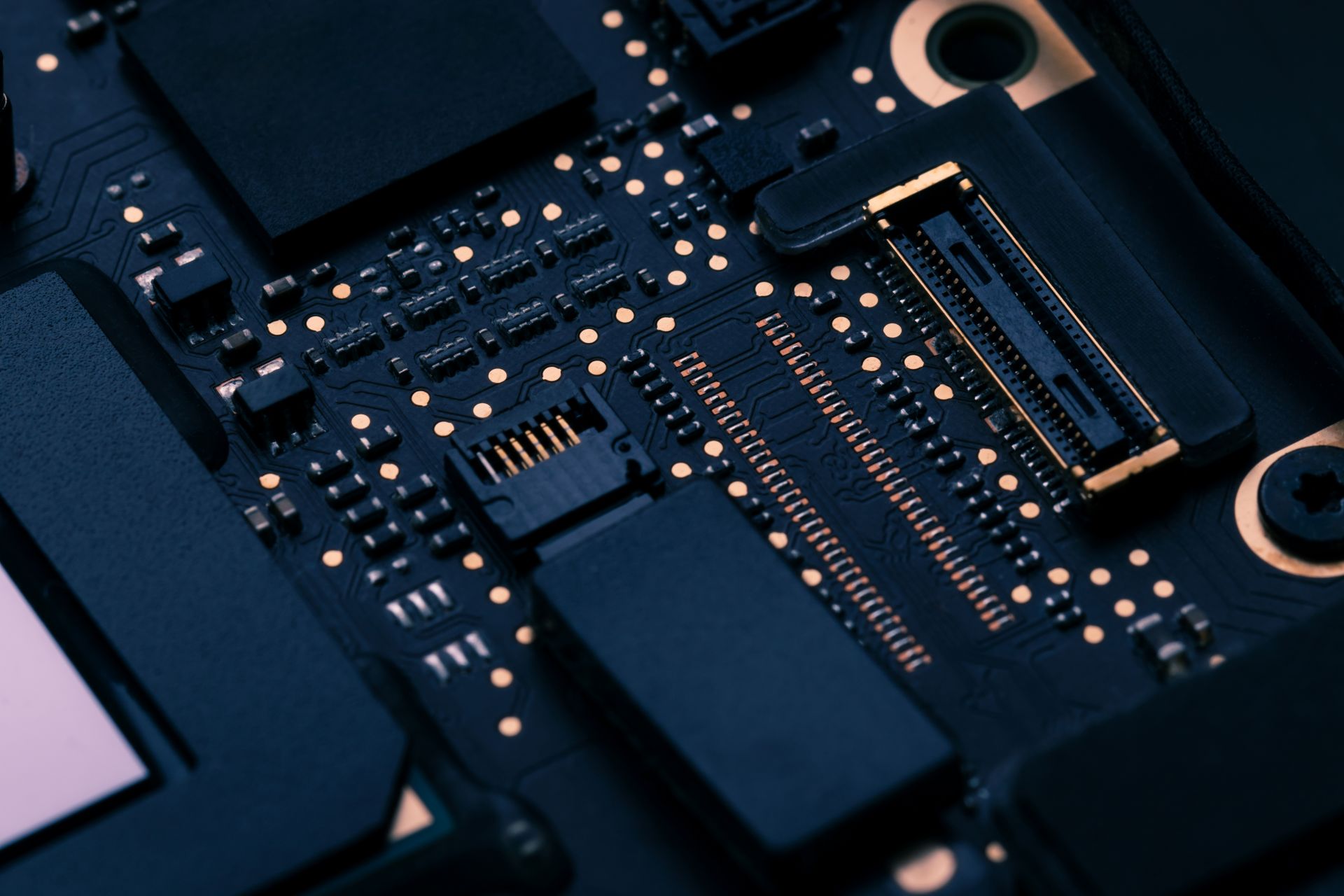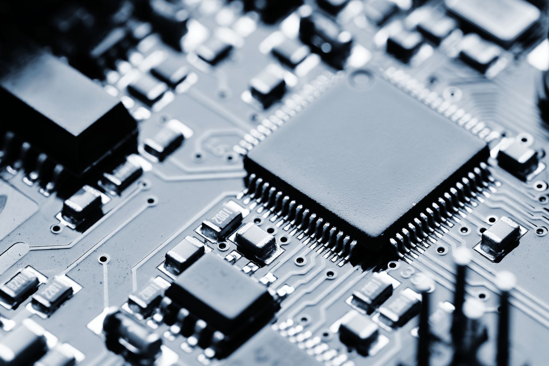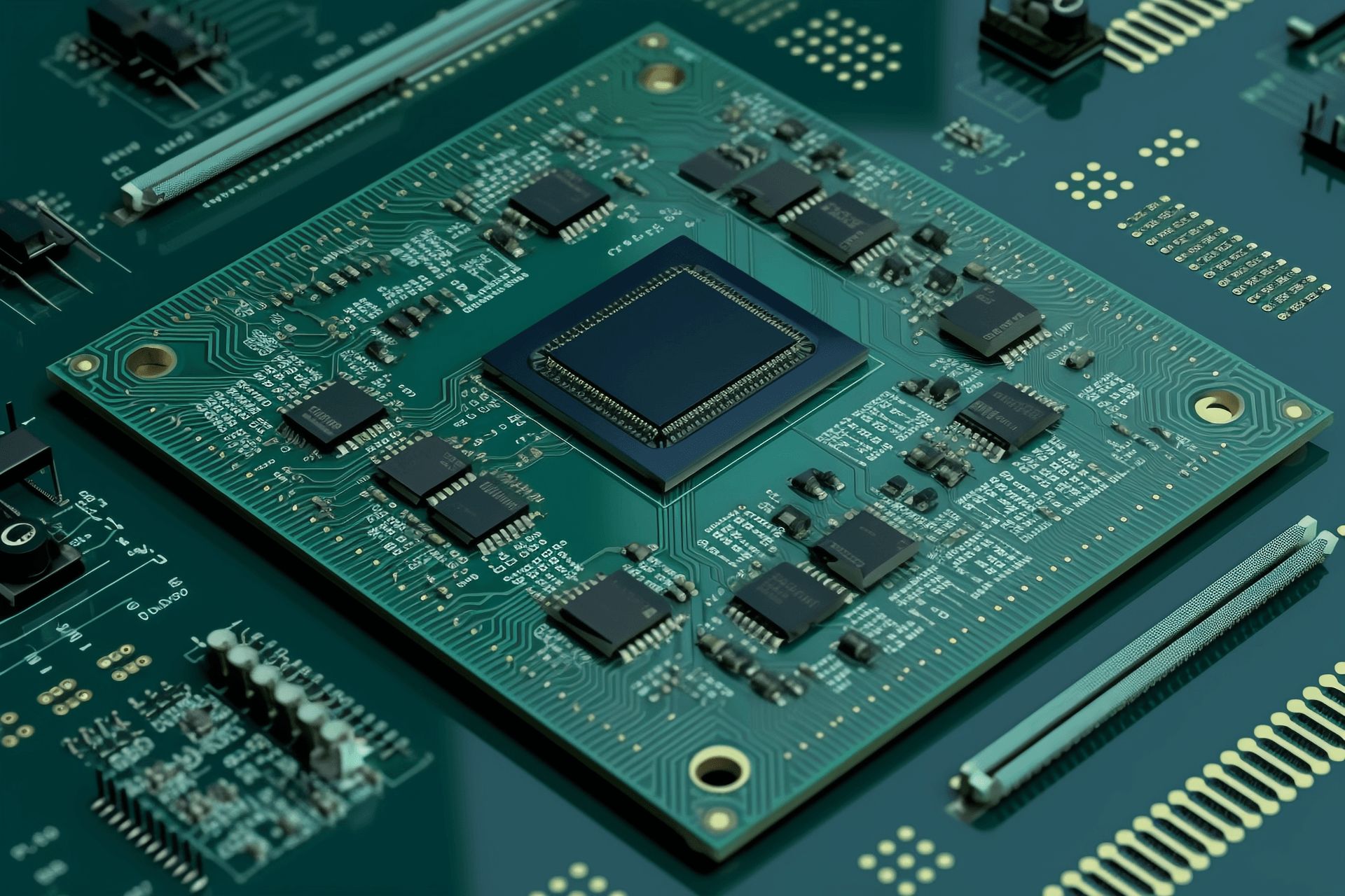
Buried via PCBs, also known as blind via PCBs, are used in various products that require high-density circuitry and multiple layers. Here are some common product areas where buried via PCBs are utilized:
Mobile Communication Devices: Buried via PCBs are widely used in smartphones, tablets, smartwatches, and other mobile communication devices. These devices often require high-density routing and smaller PCB sizes to accommodate more features and components.
Computers and Servers: Computers and servers in data centers require complex circuit layouts and high-speed signal transmission. Buried via PCBs can provide better circuit isolation and higher signal integrity to meet the demands of high-performance computing and communication.
Automotive Electronics: Modern automobiles feature increasingly complex electronic systems, necessitating compact circuit layouts and reliable signal transmission. Buried via PCBs are employed in automotive electronic modules, control units, and in-car entertainment systems.
Industrial Control Equipment: Industrial automation and control equipment often require high-density circuitry and reliable signal transmission. Buried via PCBs can fulfill these requirements, offering improved electromagnetic compatibility and noise suppression capabilities.
Medical Devices: Medical electronic devices demand compact, reliable circuit layouts, and high-speed signal transmission. Buried via PCBs are used in medical monitoring equipment, surgical devices, and medical imaging systems.
In summary, buried via PCBs play a crucial role in products that require high-density routing, complex circuitry, and reliable signal transmission. They provide greater design flexibility and performance advantages, while meeting the miniaturization, efficiency, and reliability requirements of modern electronic devices.